What Should We Do With the Inputs to Unused Logic Gates & Functions? (Part 2)
Sep 07, 2024
What Should We Do With the Inputs to Unused Logic Gates & Functions? (Part 2)
Before we plunge headfirst into the fray with gusto and abandon (and aplomb, of course), let’s remind and reassure ourselves that—although the following discussions focus on the devices and technologies that were prevalent in my youth—many of the concepts presented here are applicable to today’s devices and technologies.
When I took my first tentative steps on the path that would lead me to become one of the leading electronics and computer engineers of my generation (at least, according to my dear old mum), it was at the height of the era of 7400-series TTL and 4000-series CMOS devices. These featured suites of predominantly 14-pin and 16-pin packages, the majority of which contained a handful of primitive logic gates (NOT, AND, OR, NAND, NOT, XOR, and XNOR) or one or more slightly more complicated functions (multiplexers, decoders, flip-flops, etc.).
Our designs could employ thousands of these gates and functions, which meant our printed circuit boards (PCBs) could end up containing hundreds of these simple silicon chips. Almost invariably, this led to a handful of gates and functions being completely unused. For example, we might require only four of the six NOT gates in a 74x04 package or only three of the four 2-input AND gates in a 74x08 part.
In Part 1 of this 2-part mini-series, we considered what to do with unused single-input gates, such as of NOT (inverter) and BUF (buffer) functions. We came up with seven options, which could be boiled down to: (a) do nothing, (b) attach pull-up or pull-down resistors to the unused inputs, and (c) connect the unused inputs directly to the power or ground rails/planes.
Also in Part 1, we discussed the values of the pull-up and pull-down resistors to be employed, which could be 1 kΩ to 10 kΩ, 2 kΩ to 10 kΩ, 1 kΩ to 4.7 kΩ, 10 kΩ to 100 kΩ, or 10 kΩ to 1 MΩ depending on the technology.
As a point of interest—and to provide a point of discussion—I have one friend who always uses 4.7 kΩ, 47 kΩ, or 470 kΩ (depending on the technology) for his pull-ups and 2.2 kΩ, 22 kΩ, or 220 kΩ (depending on the technology) for his pull-downs. He does this because it allows him to quickly spot his pull-up and pull-down resistors, and who amongst our number can argue with logic like that?
One final point of interest that—for reasons discussed in Part 1—in the case of regular TTL inputs, it’s preferable to use a pull-up resistor to the power plane/rail because the gate will consume a tiny bit less power than if we used a pull-down resistor to connect the input to ground.
Following the publication of Part 1, several members of the Design News community emailed me to say: “Never leave unused inputs unconnected, especially with CMOS!”
Another reader emailed me to say: “Ideally, the input(s) should be pulled such that the output(s) drive low (logic 0) values due to EMC considerations. This is because a high (logic 1) on an output could become an emitter of ripple/variations of the supply voltage. A low (GND) is generally considered to be more stable. In automotive designs, for example, it is recommended to drive all unused outputs to low (GND) to minimize emissions.
So, this leads us to our first conundrum. In the case of a regular TTL NOT gate, using a pull-up satisfies both criteria in that it minimizes power consumption and drives the output to logic 0. But what about a BUF gate (which is implemented inside the device using two NOT gates in series)? In this case, using a pull-up on the input will result in a logic 1 on the output. Alternatively, using a pull-down on the input to generate a logic 0 on the output will consume fractionally more power. Which is the best option? I don’t know for sure. (Do you?)
Happily, this conundrum doesn’t apply to CMOS logic gates because there is no power difference between using a pull-up or a pull-down, so we can deploy whichever we need to generate a logic 0 on the gate’s output.
Before we proceed to the next topic, while still contemplating single-input logic gates, we might ask ourselves if there are any special pull-up vs. pull-down considerations when using BUF or NOT gates equipped with Schmitt trigger inputs. This is another poser for which I’m obliged to say: “I don’t have a clue.”
A quick reminder
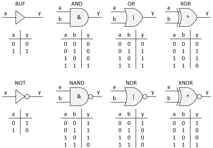
The following diagram is offered as a quick reminder for any beginners to digital logic who are perusing and pondering this column.

Symbols and truth tables for simple logic gates. CLIVE "MAX" MAXFIELD
Also, with beginners in mind, it may be worth noting that lecturers usually start off with the simplest gates (BUF and NOT). Next, they introduce the non-inverting multi-input gates (AND, OR, and XOR), and they then move on to the inverting multi-input gates (NAND, NOR, and XNOR).
What many novices neglect to note is that it’s generally easier to create an inverting function than its non-inverting counterpart. In the case of CMOS, for example, 2-input NAND and NOR gates each consume four transistors presented as a single level of logic. To implement 2-input AND and OR gates, we attach NOT gates to the outputs of our NAND and NOR gates, respectively.
Since a NOT gate requires two transistors, this means our 2-input AND and OR gates each consume 6 transistors presented in two levels of logic. In turn, this means AND and OR gates consume more power and have longer delays than their NAND and NOR cousins. All this explains why the hand-crafted circuits of yesteryear made so much use of inverting functions (this remains true today, of course, but we don’t tend to notice it so much because design tools like logic synthesis engines take care of this sort of thing for us).
Unused multi-input gates
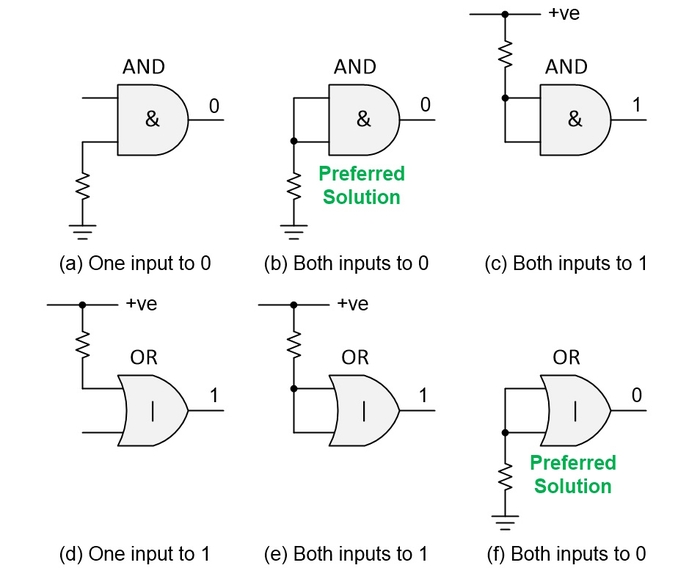
The next level in our meandering musings is to decide what to do with unused multi-input gates. Let’s start with 2-input AND and OR gates as an example. Assuming we are all agreed that doing nothing is not an option, then we have three possibilities for each gate as illustrated below:

AND and OR gates. CLIVE "MAX" MAXFIELD
In the case of the AND, we could tie just one of the inputs to GND as depicted as (a) in the figure, because any 0 on an input will force the output to 0. On the other hand, some engineers say that the unconnected input may build up electrostatic charge that could end up damaging the chip or nearby devices. Other engineers say that the unconnected input can act as a miniature radio frequence (RF) antenna. Are either of these really a thing? I don’t know. But this does lead us to the solution depicted as (b) in the figure, which is to connect all the inputs to GND. Since this also generates a 0 on the output, this would be the preferred solution in this case.
The remaining alternative is to connect all the inputs to +ve, which is depicted as (c) in the figure. The downside here is that we end up with a 1 on the output.
Observe that we cannot connect just one of the AND gate’s inputs to +ve because—in addition to its aforementioned potential to build electrostatic charge or act as an RF antenna—the unconnected (floating) input could wander back and forth between 0 and 1 causing the gate to switch and burn some amount of power. Even worse, in the case of CMOS, the unconnected input could hover halfway between +ve and GND, resulting in multiple transistors being (at least partially) active simultaneously, thereby burning a lot of power (relatively speaking).
In the case of an OR gate, a 1 on any of the inputs will drive a 1 on the output. It’s only when all the inputs are 0 that the output will be 0. Since we are aiming at the output of our unused gate being 0, this means option (f) in the above figure is the preferred solution in this case.
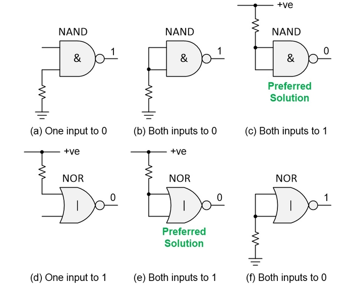
Similar considerations apply to NAND and NOR gates as illustrated below.

NAND and NOR gates. CLIVE "MAX"MAXFIELD
O-M-Gosh! When I started this column, I fully expected to wrap everything up, but I fear we’ve barely scratched the surface. We still need to consider what to do with unused inputs in the case of partially used logic gates and more complex functions.
But turn that frown upside down intro a smile because we can cover all of this in Part 3. In the meantime, do you have any thoughts you’d care to share on this surprisingly thought-provoking subject? If so, please feel free to email me at [email protected].